

Low Temperature Superconducting Device Laboratory
Development of Nb-based low temperature superconducting devices
Purpose of research
- We are developing low-Tc superconducting devices such as Single-Flux-Quantum (SFQ) circuits. Purpose of the research is developments for lower power dissipation, higher speed and more sensitive devices which breakthrough the limitations of conventional technologies.
Research themes
- JST /CREST “Low-Power, High-Performance Reconfigurable Processor using Single Flux Quantum Circuits” (FY19.4-FY24.3)
- Development of Nb-based fabrication process to build a new architecture named Reconfigurable Data Path (RDP) into SFQ circuits, and to create basic technologies for a 10 TFLOPS desk-side supercomputer whose power consumption is almost 1/100 compared with that using semiconductor technology.

An image of an SFQ/RDP desk-side supercomputer of 10 TFLOPS(JST/CREST) |
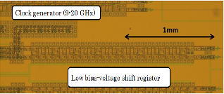
- JSPS “Research for Sub-μW Micro-Processor by Introducing Adiabatic Mode Single Flux Quantum Circuits” (FY22.7~FY27.3)
- Development of Nb-based fabrication process for reducing power consumption of SFQ circuits to 1/400~1/105 compared with conventional SFQ Circuits.
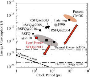
Advantages in clock speed and power dissipation of SFQ circuits and possibility of further improvement. (JSPS) |
- FIRST “Quantum Information Processing” (FY22.8~FY26.3)
- Development of fabrication process for Al-based quantum bits collaboration with National Institute of Advanced Industrial Science and Technology (AIST)
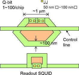
Layout example for developing Al Quantum bit (FIRST) |
- JSPS ”.Research for wide band and wide dynamic range readout circuit for multi-pixel superconductive photon detector” (FY23.7~26.3)
- Development of microwave SQUID for multi pixel superconductive detectors with AIST
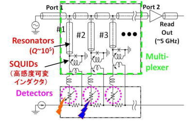
Readout scheme using microwave SQUID (JSPS) |
Main results
- Development of SFQ circuit fabrication process
- Fabrication of Nb 9-layer devices by introducing a new planarization technology.
- SFQ 2×2 RDP circuit fabricated by Nb nine layer process was successfully operated up to 45 GHz.
- Improvement of fabrication yield by figuring out causes of process defects and achievement of 70,000 JJs shift register circuit operations without any defects.
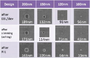
- Development of small JJ fabrication process using Chemical Mechanical Polishing (CMP).
- Development of small Al JJ patterns (as small as 30 nm Φ).
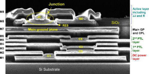
Cross section SEM image of Nb nine layer device (CREST) |
SFQ 2×2RDP circuit fabricated by Nb nine-layer process(CREST, design and measurement by Nagoya University) |
A shift-register circuit with 1/500 power dissipation. |
Al JJ patterns for quantum bits (FIRST) |
- Development of circuit design methodology for SFQ circuits
- Establishment of a cell-based design methodology for SFQ circuits.
- Development of high-speed and lossless superconducting wiring technology (PTL).
- Development of automatic design tools for SFQ circuits and demonstration of their effectiveness by designing a large-scale SFQ circuit including 400,000 Josephson junctions within 8 hours.
- Development of implementation technologies for SFQ systems
- Development of a superconducting multi-chip-module (MCM) technology which places several chips onto a carrier with superconductive wirings and experimentally demonstration of its 117 Gb/s data transfer between chips by SFQ pulses.
- Demonstration of movie data transfer between 4 PCs through an SFQ switch system cooled by a cryo-cooler.
- Success of a 40 Gb/s optical data input experiment into an SFQ circuit.
Application items
- Superconducting detectors.
- Waveform monitors for optical networks (high-speed measurement).
- Ultra low-power switches in network routers.
- Superconducting accelerators to realize smaller-size and lower-power supercomputers.
- National standards for electrical mesurements.
Key papers
- K. Hinode, T. Satoh, S. Nagasawa and M. Hidaka, “Origin of Hydrogen-inclusion-induced Critical Current Deviation in Nb/AlOx/Al/Nb Josephson Junctions”, Journal of Applied Physics, 107 p 073906 , 2010.
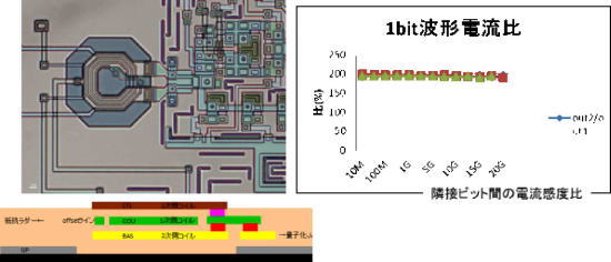
- H. Suzuki, M. Oikawa, K. Nishii, K. Ishihara, K. Fujiwara, M. Maruyama, M. Hidaka, “Design and Demonstration of a 5-Bit Flash-Type SFQ A/D Converter Integrated With Error Correction and Interleaving Circuits”, IEEE Trans. Appl. Supercond. vol. 21 no. 3, p. 671-676, 2011 .
- M. Maruyama, H. Suzuki, Y. Hashimoto and M. Hidaka, “A Flash A/D Converter Using Complementary Combined SQUIDs”, IEEE Trans. Appl. Supercond., 19, pp. 680-684, 2009.
- M. Hidaka, S. Nagasawa, K. Hinode and T. satoh, “Improvements in Fabrication Process for Nb-based single flux quantum circuits in Japan”, IEICE Trans. ELECTRON., E91-C, pp. 318-324, 2008.
Results of NEDO project finished by February 2012
NEDO “Development of Next-Generation High-Efficiency Network Device Project”(FY19.6-FY24.3)
- Targets
- Superconducting real-time oscilloscope to observe high-speed waveform in optical communication network by using SFQ devices which are the ultimate high-speed and low-power-dissipation ones.
- Development of SFQ high-speed Analog to Digital Converter (ADC).
- 5-bit ADC with sampling frequency of 50 GS/s.
- Input band width of 25 Gbps.
- Improvement of SFQ circuit fabrication process.
- Increase of Jc and improvement its controllability.
- High-speed assembly into a cryo-cooler for mounting the ADC chip.Optical input to SFQ circuits.
- Optical input to SFQ circuits.
- Results
- Achievement of 50 GS/s (50 GS/s × 1) 5-bit ADC by adoption of a complimentary combined SQUIDs and increase of Jc.Increase of input bandwidth
- Increase of input bandwidth to 26 Gbps by improvement of input trance.
- Development of high-speed assembly and demonstration of SFQ circuit operation by 40 Gbps optical input.
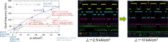
(left fig)Estimation of sampling frequency of SFQ ADC.( Jc: Critical current density of JJ) |
Achievement of 50 GS/s by Jc increase |
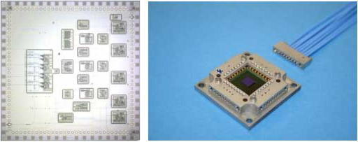
SFQ ADC chip and cryo-package for mounting to cryo-cooler |
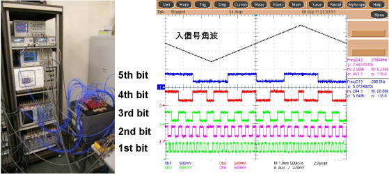
(left fig)Measurement setup for SFQ high-speed ADC with cryo-cooler. |